Using GPS on RISC OS Part 5 - Additional information
A series of articles has been published in Archive Magazine describing the design and construction of a GPS receiver and speedometer:
- In part 1 (Archive 24:2) I described a Raspberry Pi that could be carried around: instead of a mouse and monitor it had an Adafruit touchscreen that just plugged in to the HDMI and USB sockets. It had a GPS module sending position data to the mapping application (RiscOSM) by means of URI_Dispatch messages generated by the !Satnav application. It thus provided a rolling map of your location using Open Street Map data.
- Part 2 (Archive 24:3) described version 1.08 of Satnav, which could control a small text display or an OLED display and could talk to RiscOSM using Wimp messages.
- Part 3 (Archive 24:4) adds a Witty Pi for control of power consumption. Satnav is at version 1.40 and can control an ‘electronic ink’ display (Papirus).
- Part 4 (Archive 24:5, October 2019) adds an Adafruit power-boost board to extend battery life, an Adafruit ADS1015 ADC board to provide battery management, improved odometer function, and adds software-controlled power-switching. GPX logging, rather than Anquet AEF format, internationalizes Satnav, now at version 1.80. At each stage the hardware has become smaller.
- Part 4 of this series was written in May 2017, updated in August 2018 and published in October 2019. The last version described had many flying wires to connect the various boards and push buttons together. It had a digitial voltmeter which, on the press of a button, would show the battery voltage, from which its remaining life could be inferred.
- Part 5 was sidetracked by an article (Archive 24:6, July 2020) which described an improved version of the power control circuitry but focused on the construction of the case for Éa small portableæ. It included the circuit diagram for power control and mentioned the use of an Adafruit ADS1015 4-channel analogue to digital conversion board.
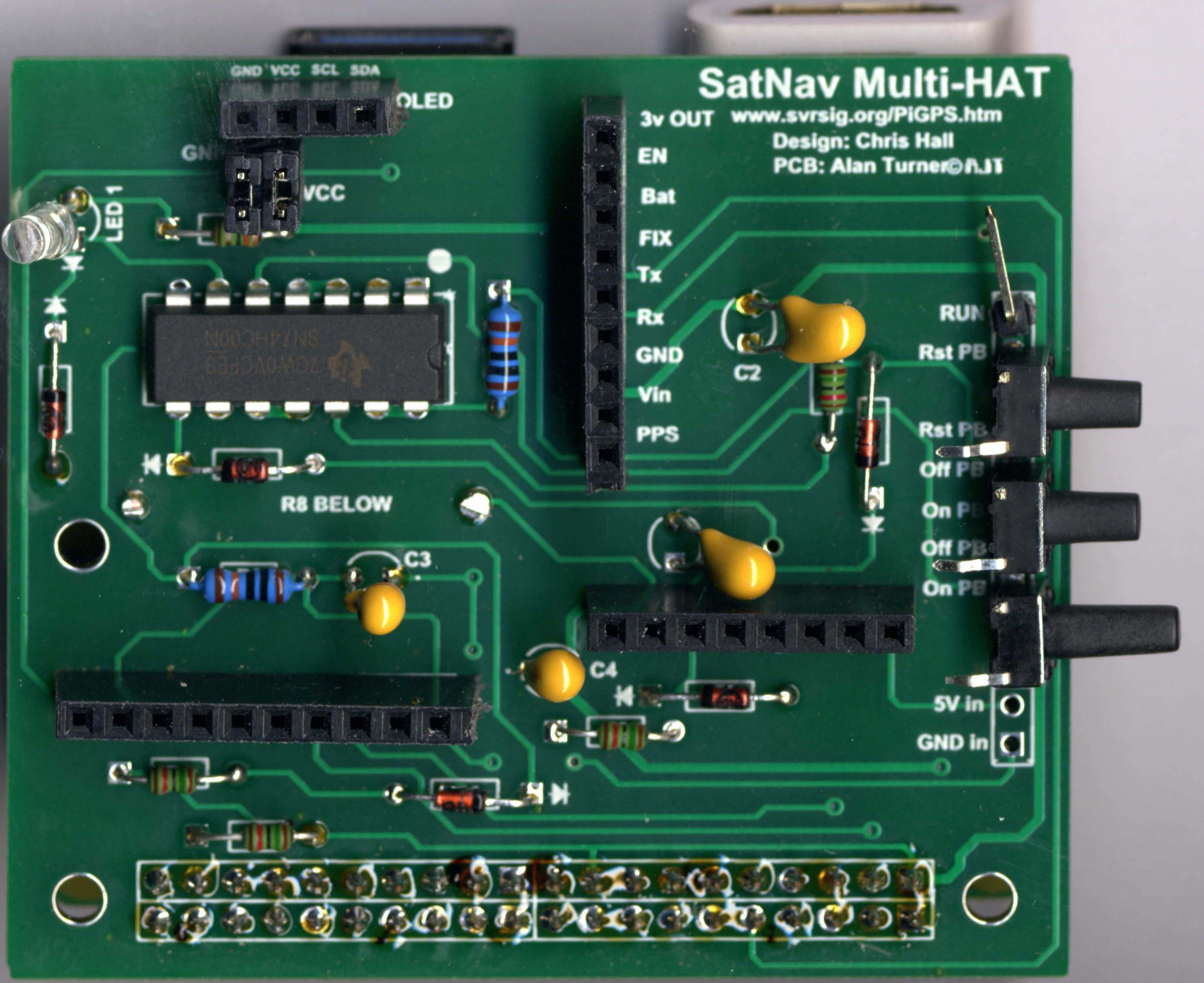
- Meanwhile I consolidated all the various different boards onto a single HAT board which is a GPS board with some breadboarding space. It adds current monitoring so as to provide a battery endurance figure in hours at the current rate of consumption. This was a bit of a hack as it involved intricate wiring. I have now obtained a purpose-built circuit board which makes the task of wiring it up much easier. Satnav is now at version 2.50.
- Some of this information is available here.
- Further information to conclude the series is given below.
Background
The last version that I described (in Archive 24:5) had many flying wires to connect the various boards and push buttons together. It had a digitial voltmeter which, on the press of a button, would show the battery voltage, from which its remaining life could be inferred. A rather primitive power control circuit using transistors was shown.
An article in Archive 24:6 described an improved version of the power control circuitry but focused on the construction of the case for Éa small portableæ.
So whatæs new?
The main improvement is to make better use of the ADC (analogue to digital convertor) board. By monitoring current consumption and battery voltage, the remaining battery capacity can be shown as a percentage and as an endurance time in hours. The board also measures the voltage of the cell on the GPS module and of any external power source.
The other improvement is to use a different GPS module (functionally identical but in the form of a HAT - Hardware Attached on Top). This allows all of the circuitry and switches to be mounted on a single ÉHATæ board with no flying leads.
Previously there were five boards connected by flying wires:
- GPS module;
- OLED display;
- Power boost board;
- ADC board;
- Breakout board for power control.
A further development was the use of a purpose-built circuit board,
The ÉHATæ board could then be tested with no ancillary boards plugged in (supplying power directly to the micro USB socket on the Pi Zero). Each board could then be added in turn and tested individually.
Circuit board construction
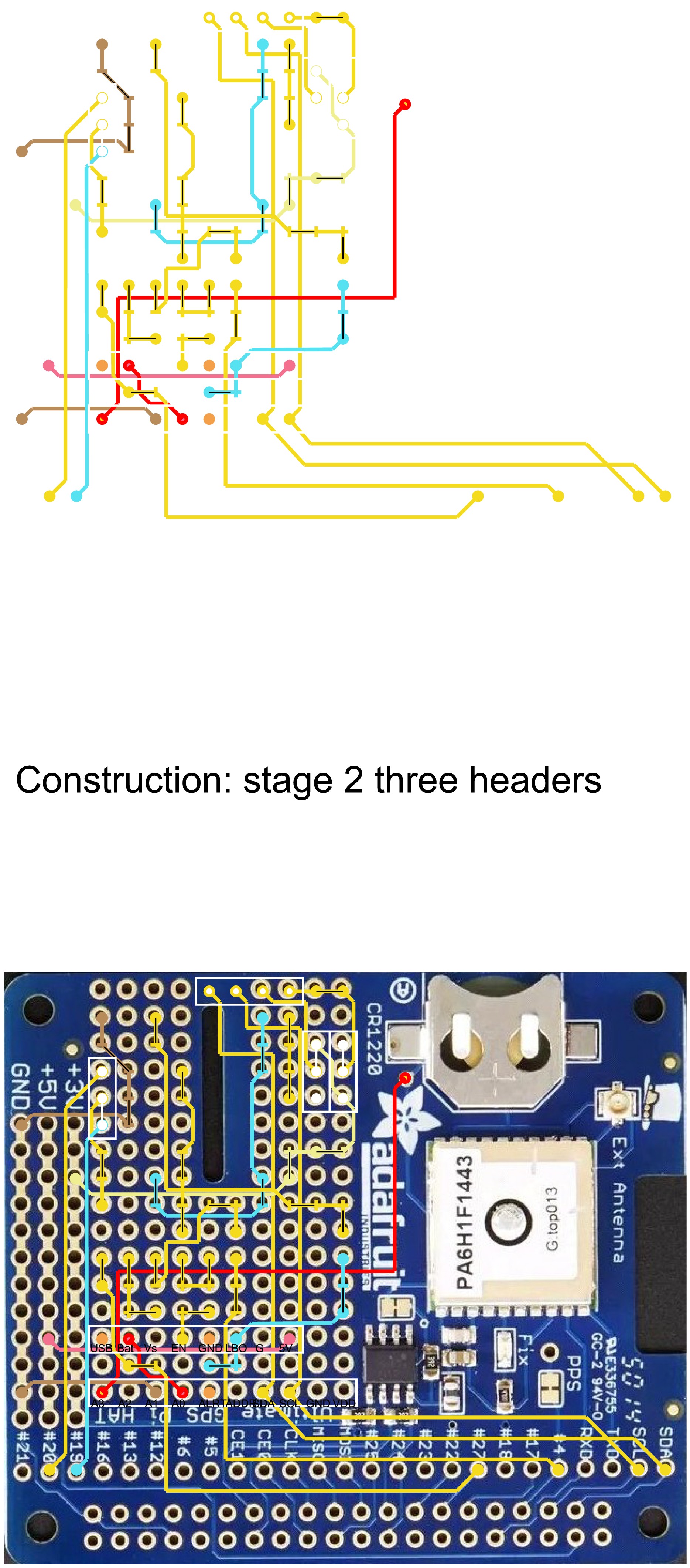
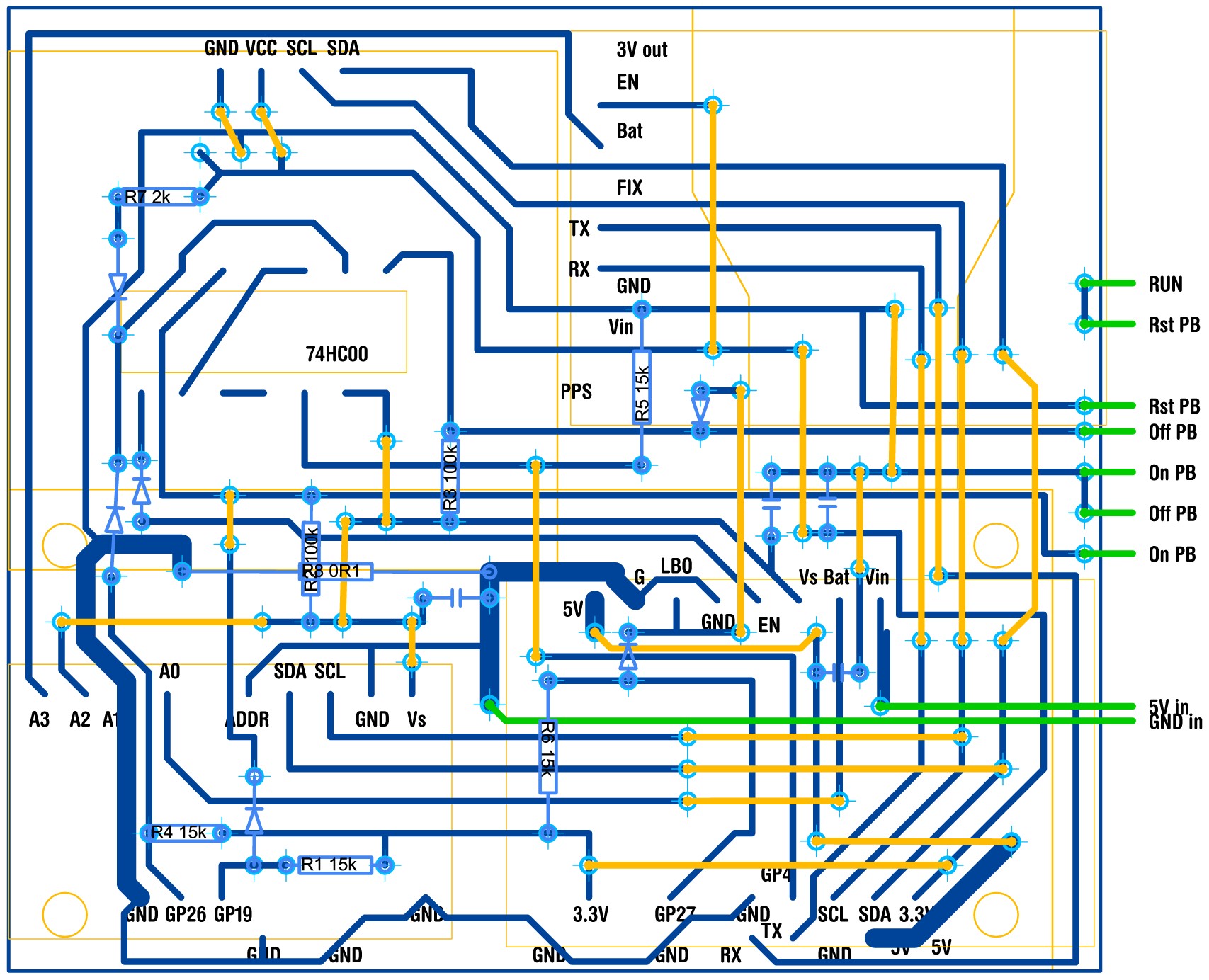
There are a lot of components on the ÉHATæ board and construction is broken down into two principal stages.
Stage 1 is to fit all of the point to point wire links (using quite small wire) that connect to the various sockets. All of this can be done underneath and out of sight. At this point the top surface will have only three sockets (OLED, ADC and Powerboost) and the bottom surface one socket (for the Pi Zero). It will also have one Éplugæ, extended header pins 1 to 6 on which a real time clock module could be fitted.
 The interconnecting wires are laid out so that a bare wire goes through each hole where a component such as a resistor, I.C., capacitor is to be fitted and is terminated each end at a soldered connection either on a header socket pin or in an otherwise unused hole. That way there are no loose connections or unsoldered holes except where components will be placed later. Where the connecting wire has a black stripe it is on the top surface, otherwise it is on the underneath. Unsoldered holes are shown with a horizontal or vertical cross line.
One or two connecting wires are more awkward and these are shown in a separate view.
 The interconnecting wires shown here are either split into several parts or take an awkward route amongst other wires. Shown separately they can be double-checked before soldering.
Continuity checks can then be done whilst working from the uncluttered top surface and a photograph taken and checked before embarking on stage 2.
 A scan part way through fitting the connecting wires on a slightly earlier design. It is reversed left to right to allow easier comparison.
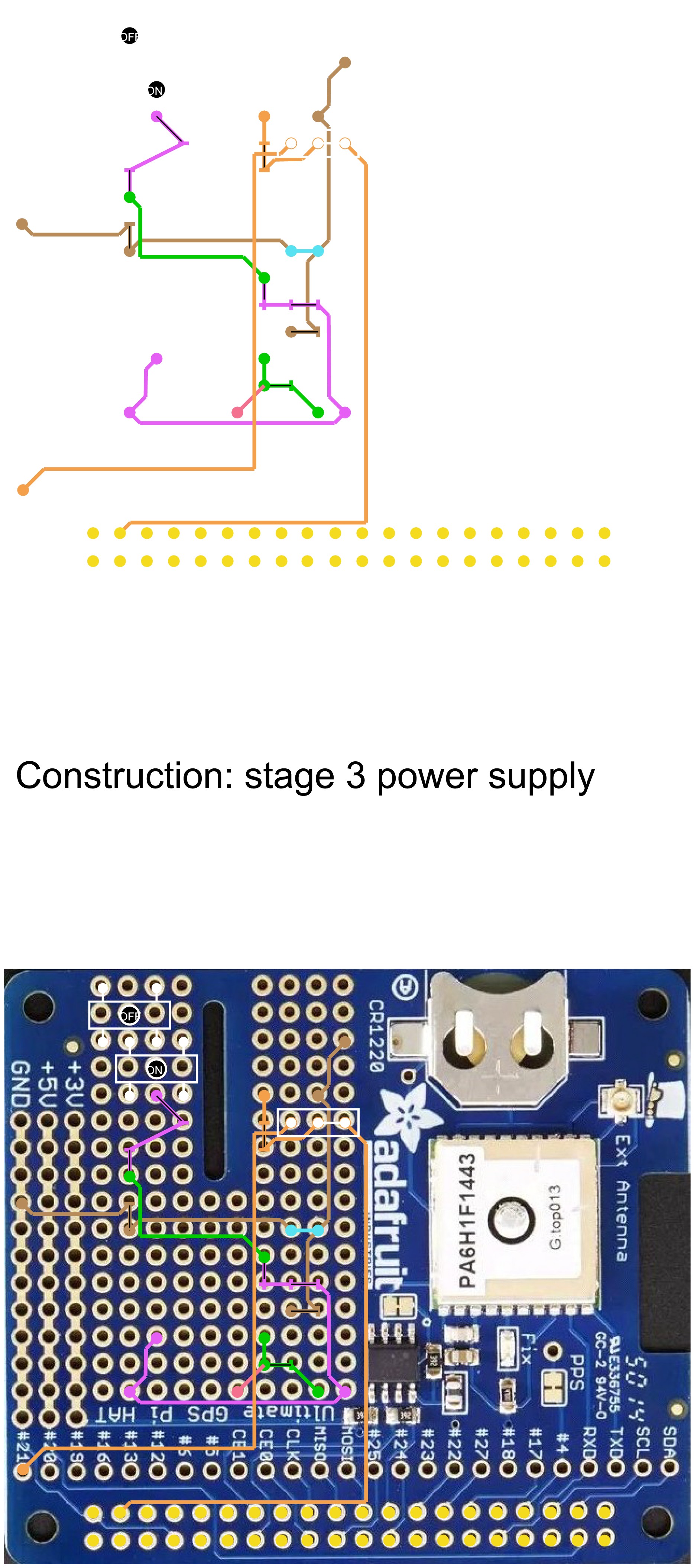
Stage 2 is to fit the resistors, 74HC00 I.C., switches, headers, diodes and more point to point links. Most of these can be mounted underneath, with the exception of the I.C., LED, headers and switches.
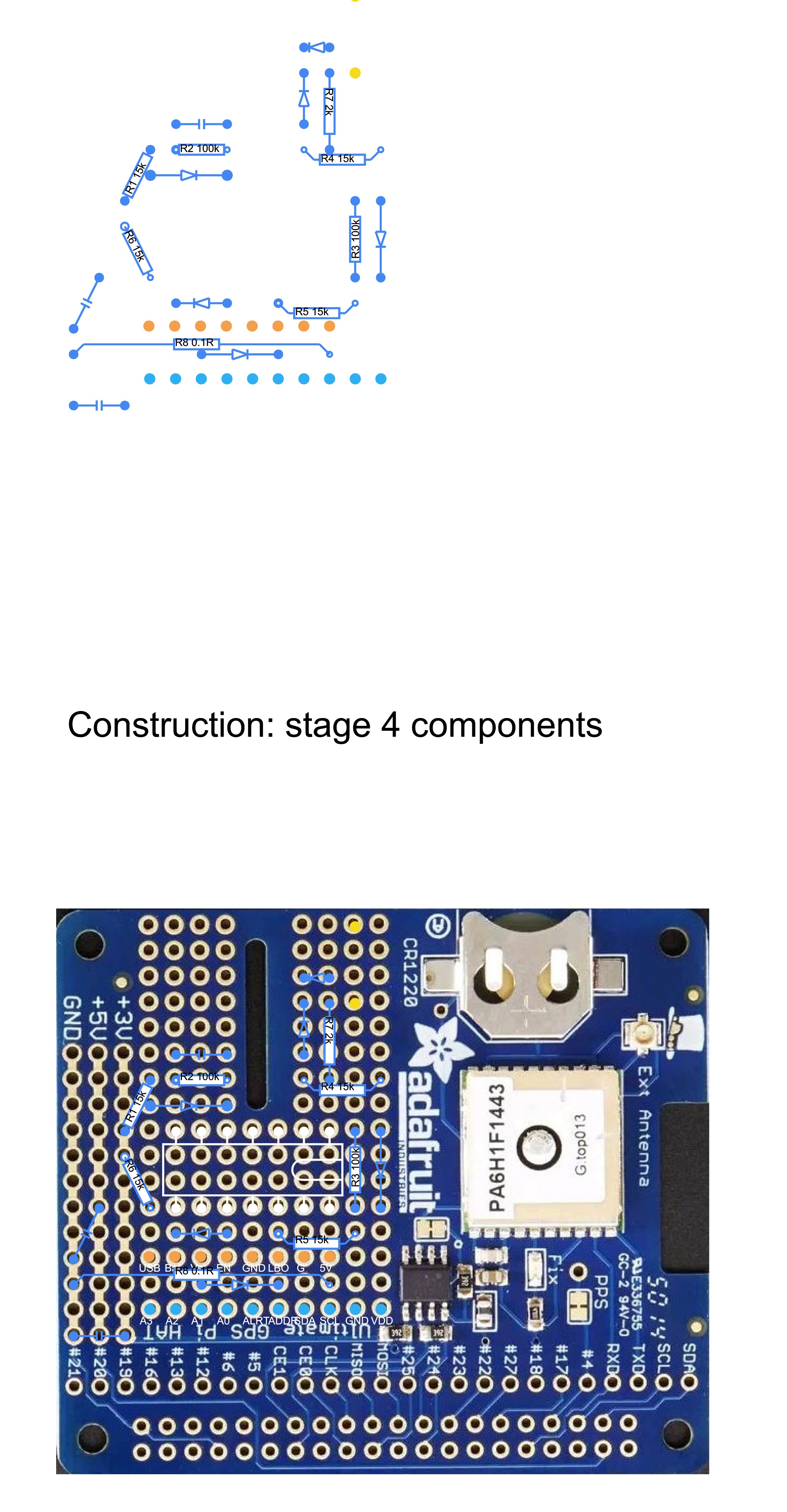 The components shown without the connecting wires. Each lead should correspond with a hole containing a bare wire passing from top to bottom.
Construction drawings
The construction process is made easier by the overlay drawings which show each stage of the circuit being laid out on the prototype board. By prefixing selective parts of the drawing process with PROCly(n) various versions of the drawing are produced. The procedure is first called with an argument of 0 which initialises it.
Each call remembers the point in memory to which draw data had been accumulated and the previous argument. If the previous argument was for a layer other than the current one, then the data pointer is restored throwing away the data accumulated since the last call.
The practical effect is that the block following a call will only be drawn if it is intended for the layer being drawn. This allows all of the variables to have their correct values whether or not the bits they apply to are being drawn.
FOR zi%=1 TO 10
PROCmdReinitialise(bfsz%-10000, bfmd%)
layer%=1<<(zi% DIV 2) OR ((1<<(zi% DIV 2))-1 AND (zi% AND 1)<>0)
PROCly(0)
PROCly(4)
PROCdrawstage2
PROCly(2+4)
PROCdrawstage1
PROCly(32)
PROCdrawlabels
PROCmdSaveDiagram(ĢDrgĢ+STR$~(layer%))
NEXT
:
DEFPROCly(test%)
IF test%=0 THEN
ptest%=0
ELSE
IF (ptest% AND layer%)=0 AND ptest%<>0 THEN _mdBufPtr%=pmdp%
ENDIF
pmdp%=_mdBufPtr%
ptest%=test%
ENDPROC
The programme above is part of that used to generate the different layers, each being a separate Draw file.
Working backwards
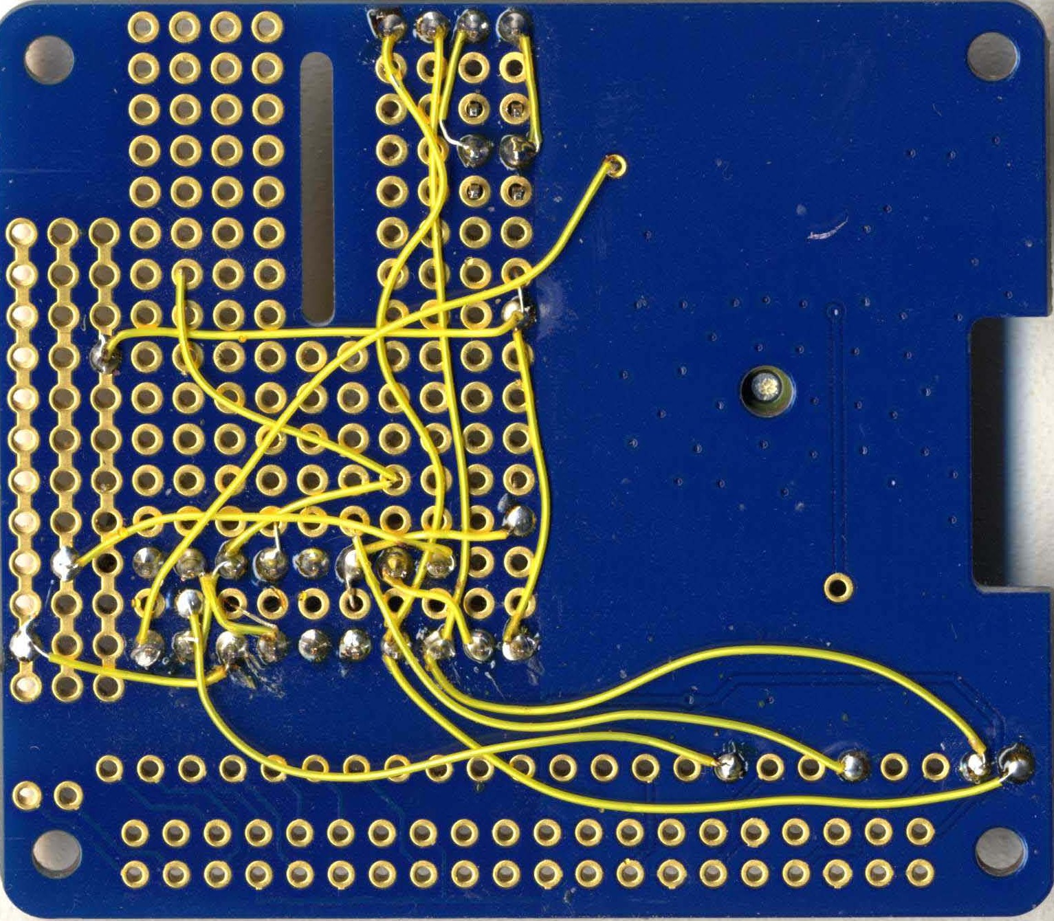
Wiring the links on the underneath (which is much neater but not originally intended) proved to be a real pain. Counting carefully was just not good enough and several times I had to unsolder a link and move it!
Checking is greatly facilitated by taking a scan once the first stage is complete. Reversing the scan from left to right then gives an image that can be checked directly against the plan.
The diagram and photo above should therefore be compared: there are several links soldered at only one end because further components are to be added and the thin connecting wire will fit into the same hole as the componentæs lead. The picture is of a slightly earlier design so the two are not directly comparable.
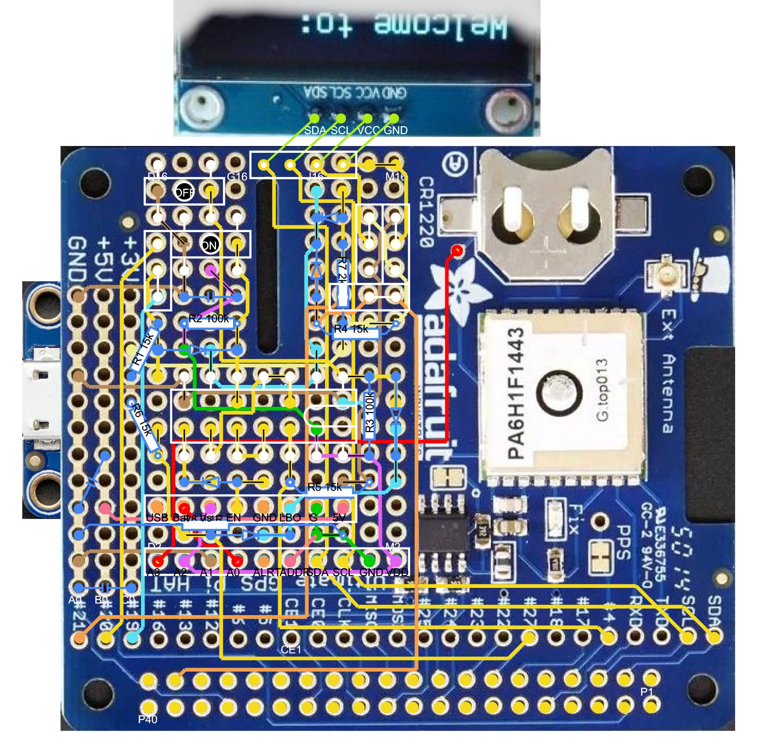 How the finished item should look: there are headers to allow OLED displays with reversed power supply pins to be used. Also GP20 may be used as an alternative to GP19 and GP21 as an alternative to GP26.
Now I reach the awkward conclusion that the 4-pin header for the OLED display would be best moved two holes further over so that an HDMI adapter can fit alongside it. That would make room for an HDMI and a USB socket, one each side of the OLED display.
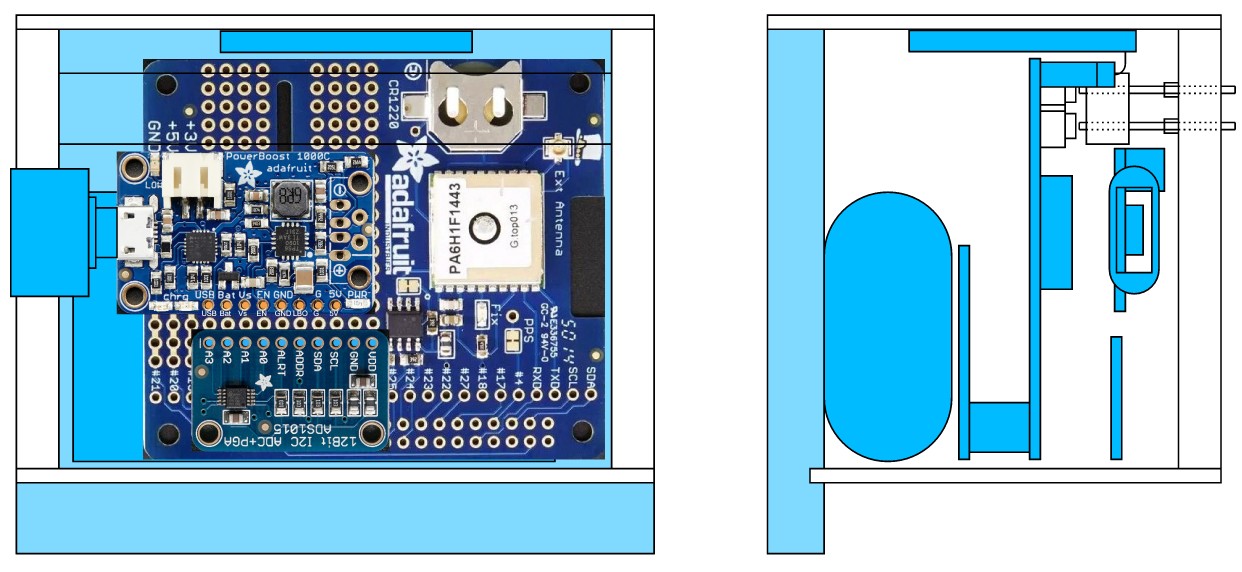 The case showing how the boards and battery are arranged.
The top will have a paper insert just underneath the top sheet, with holes for the various indications to shine through. Thus the indications will be labelled with their various meanings.
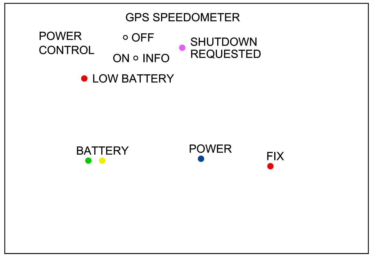 The paper insert for the top cover.
The side panel will need holes for the short batten that guides the Éonæ and Éoffæ shafts and a cut-out for the USB socket, see above.
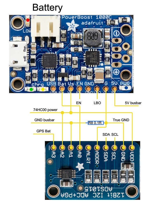
ADC module & 74HC00 chip
The Adafruit ADS1015 4-channel breakout board is ideal for adding high-resolution analogue to digital conversion. It must be powered between 2V and 5.5V and at a voltage at least equivalent to the highest voltage it is monitoring. Otherwise it will back power its supply rail via its protection diodes. The 74HC00 chip can be powered at between 2V and 5V and controls power supply switching. Both must therefore be powered continuously.
The circuit diagram for power control. The resistor R7 and LED ensures that the initial condition when powered up is 'OFF'.
The power boost board features two DC to DC convertors - one to charge the battery from the external source and another to provide 5.2V power which takes its input, via switching diodes, from either the external power source or the internal LiPo battery, whichever is the higher voltage. This voltage, about 40mV below battery voltage when there is no external power supplied, is available as an Éalways onæ power source. This difference of 40mV is within the maximum rating of 300mV above supply voltage.
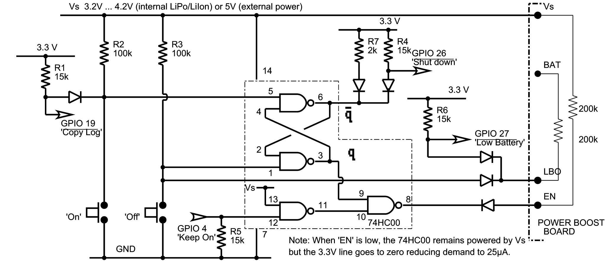 The connections for the power supply are arranged to allow the current consumption to be measured as a small voltage drop in the ground connection.
Testing
I particularly wanted to test the ADC module which is supplied at 5V but 3.3V logic is used for the IIC lines - these are driven to low but go high with pull up resistors. Logic high is defined as at least 70% of the power voltage which means between 3.5 and 5V. I am hoping that 3.3V will prove OK as logic high (inactive). It did.
This will allow me to measure voltages directly (the input impedance of inputs A0 to A3 is 10MW at a FSD of 6V and 100MW at a FSD of 256mV) rather than via a resitive divider circuit.
Current measurement
The ADC board and 74HC00 chip are powered directly from the power boost board but the other components are supplied at 5.2V from the main output of the board via a simple series resistor of 0.1W in the ground leg, as shown above. This causes the GND busbar to be at a small voltage above true ground which can be measured to indicate current consumption. The 12 bit resolution of the ADC1015 will measure up to 256mV at ▒60ĄV (current up to 2.56A ▒ 0.6mA).
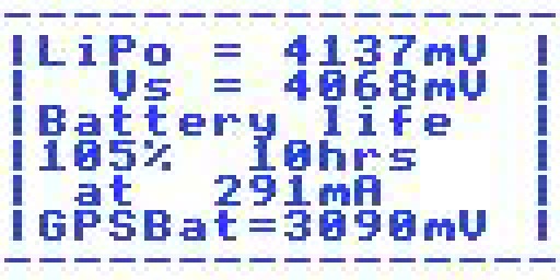
The battery has just been fully charged and shows 10 hours life with a keyboard and mouse connected.
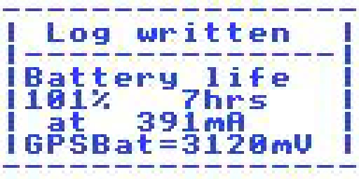
The current comsumption increases as a USB flash drive is inserted and a download requested (the same button shows battery condition and requests a download).
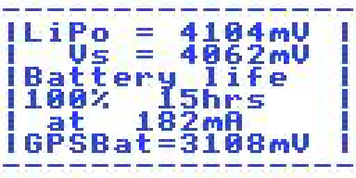
With no USB connection, current consumption dropos and a lifetime of 15 hours is shown.
Power consuption changes markedly depending whether a USB hub with keyboard and mouse is connected and whether a USB pen drive is connected, see below.
Powering off
Once the components have all been incorporated, the power boost board can be fitted. The flip-flop circuit controls the power and its status can be read by GPIO pins 19, 26 and 27. This allows a shutdown request to be detected, as well as a low battery condition. It also allows the Éonæ button to be used as a request to download or show data. So a journey log can be downloaded to a USB stick or the battery status displayed by the readings taken by the ADC module.
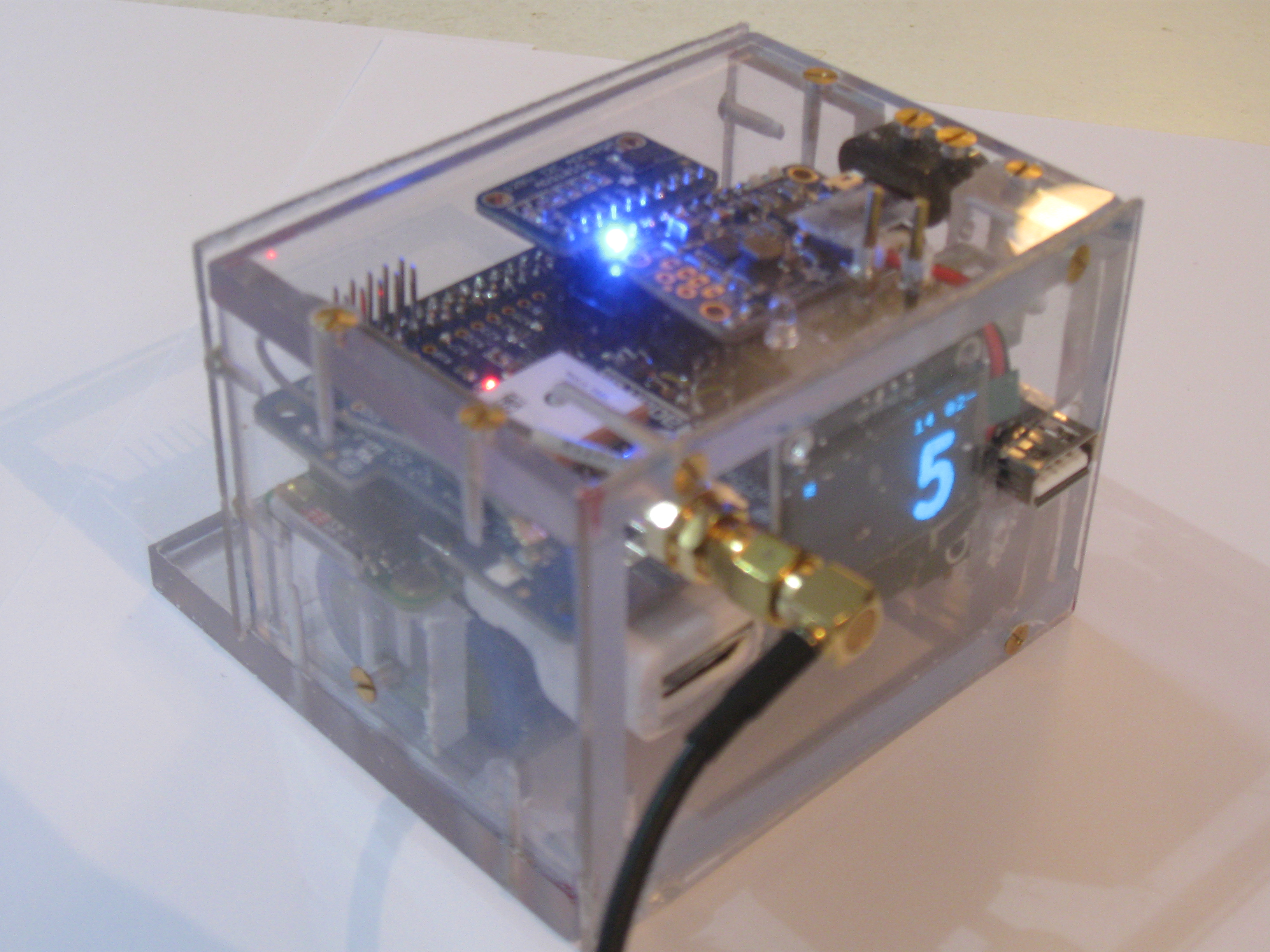 The finished unit showing a speed of 5 mph. The external antenna is fitted but there are no other connections.
Looking at the circuit above, a low battery condition forces a shut down request so that both GPIO 26 and 27 go low and the Éshutdown requestæ LED lights. This is detected by software and once logging is complete, a shutdown is forced by a software reset. As the computer shuts down, GPIO 4 goes to a high impednace state once the OS has written to CMOS and shut down any running applications. The ÉENABLEæ line is taken low and power is removed, leaving only the 74HC00 chip and the ADC1115 chip powered. The combined load they present during shutdown is 25ĄA.
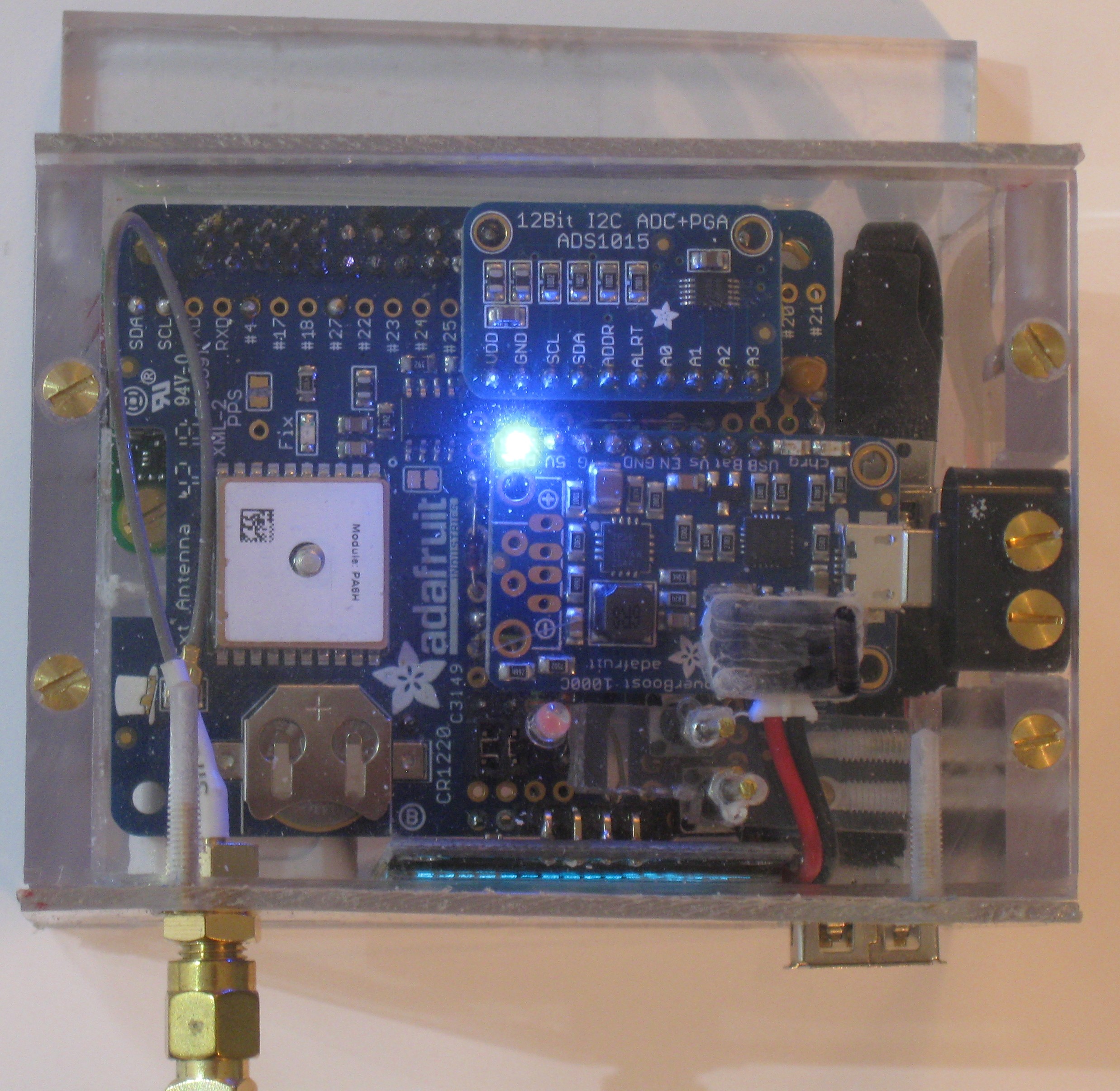 The finished unit looking from the top.
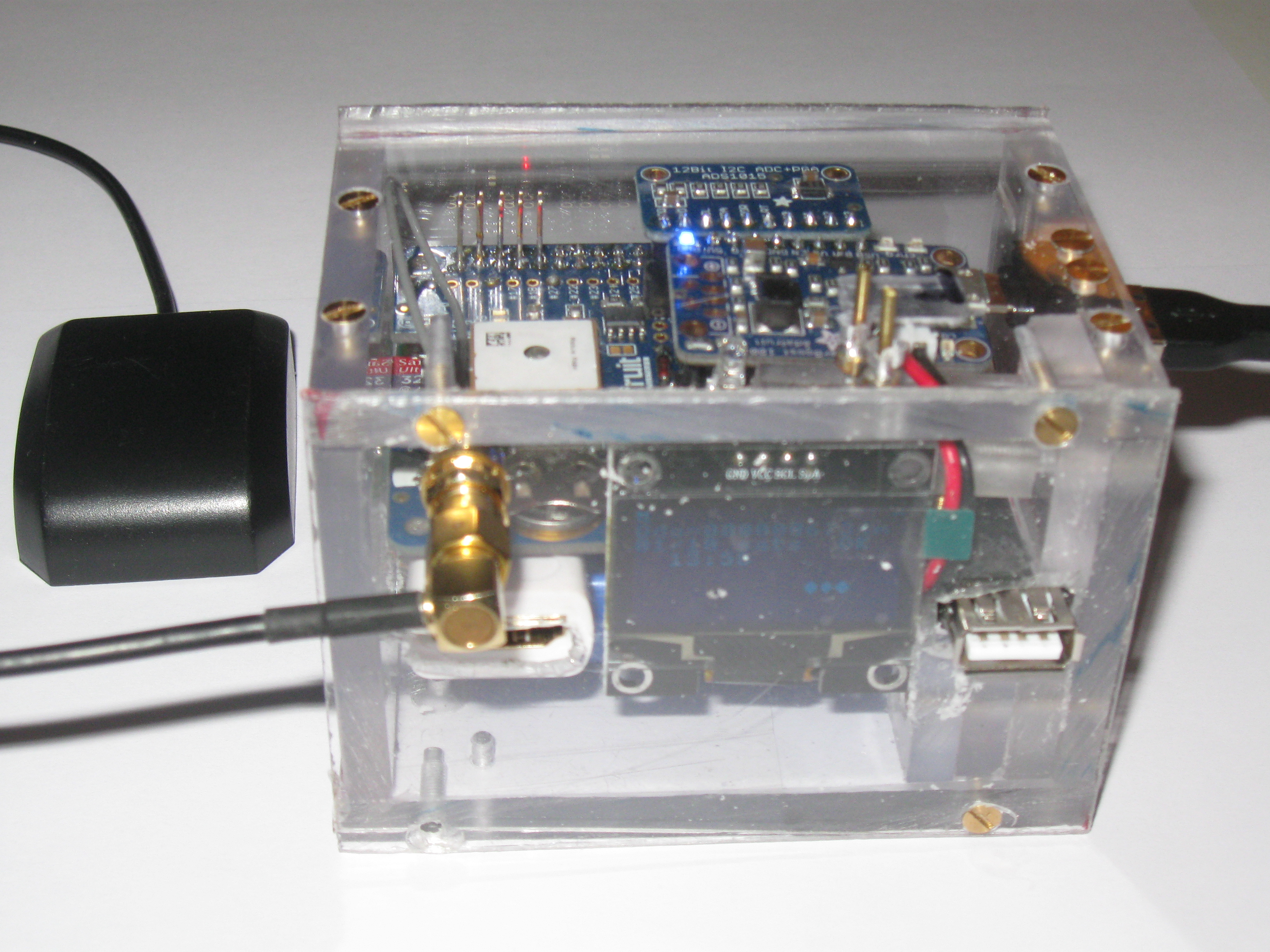 The finished unit looking from the front.
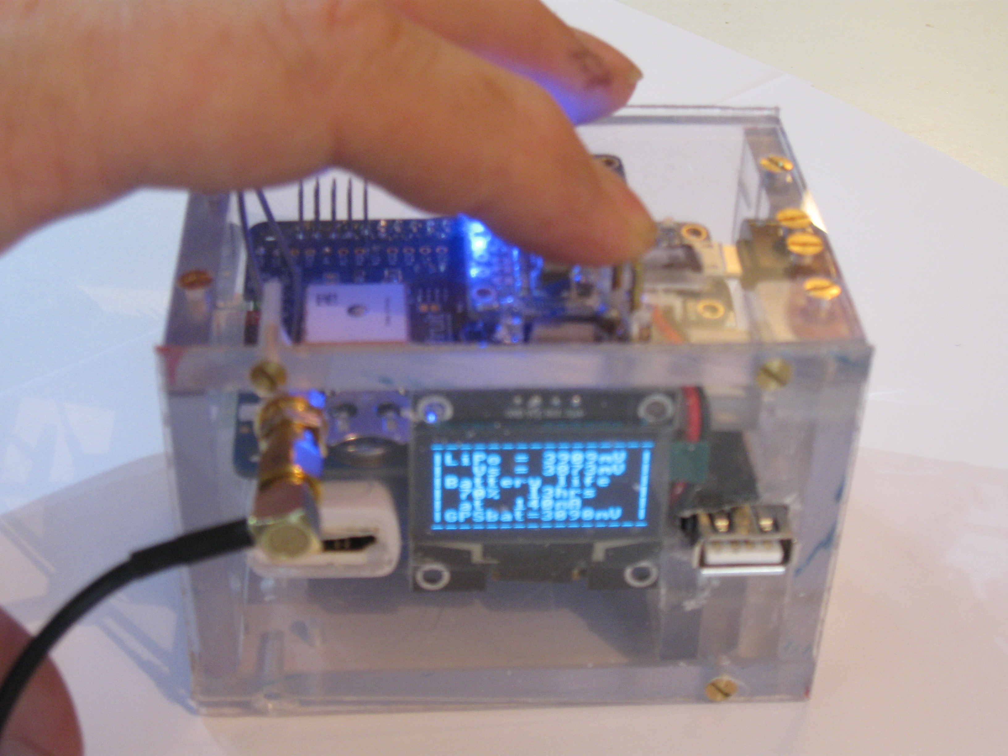 The push buttons on the circuit board are operated by small rods - here the 'INFO' button is being pressed to ask for the battery condition to be shown.
Final testing
SatNav version 2.20 (Aug 2018) just worked with only minor bugs (now corrected in version 2.50). The battery capacity is calculated from the battery voltage and this is also shown as hours remaining at the measured current consumption.
It took longer to construct than I expected as I had to work from the underside of the board where it was a mirror image of the diagram I was working from. A few errors crept in and had to be corrected.
Final innovation
At each stage the hardware has become either more compact or more functional but each time has been based on a breadboarding style where a bespoke circuit is constructed. Some items such as a liquid-ink display or use of the Witty Pi to turn the unit on after a prescribed time have proved an unnecessary refinement.
Different breakout boards have been used - ProtoPAL, Zero Breakout as well as a GPS board with some breadboarding space. I have also used a Witty Pi board to allow a shutdown unit to be reawakened at a specific time and date.
The final version now uses four plug-in modules: a GPS module which deals with the satellite GPS signals; an OLED display module which provides a display in lieu of an HDMI monitor; an analogue to digital module which allows voltages to be measured and a power boost board which allows the unit to be run from a battery.
The problem with a breadboard approach is that wiring it up is tedious and error prone. Previous versions used intricate wiring on a breadboard that required enormous patience (not my strong point) and much correction of minor wiring errors. It is a good approach while each unit is breaking new ground but once a design is finalised there is a huge advantage in moving to a custom PCB.
I worked out that there was (just) enough space on a 68mm x 60mm PCB to mount all four modules, each with a header socket and the few components with plenty of space around each for soldering. I designed this to be a Émulti-HATæ board, accommodating the four modules and plugging in to a Pi Zero.
 The original rough layout for the PCB, put together manually using MakeDraw.
I laid out an approximate design for the PCB on 28 April 2022 and with some considerable help from a colleague who knew how to specify PCBs we reached a concensus on the design (version 7) by 4 May and I ordered it from China the same day. It was delivered on 9 May. Pretty good service!
 The original rough layout for the PCB, put together manually using MakeDraw.
The ÉMulti-HATæ board can now be tested with no ancillary boards plugged in (supplying power directly to the micro USB socket on the Pi Zero). Each board could then be added in turn and tested individually.
 The original rough layout for the PCB, put together manually using MakeDraw.
More testing
The power boost board features two DC to DC convertors - one to charge the battery from the external source and another (controlled by the Éenableæ input EN) to provide 5.2V power which takes its input, via switching diodes, from either the external power source or the internal LiPo battery, whichever is the higher voltage. This voltage, about 40mV below battery voltage when there is no external power supplied, is available as an Éalways onæ power source from the internal battery.
The ADC board must be powered at between 2V and 5.5V and at a voltage at least equivalent to the highest voltage it is monitoring. Otherwise it will back power its supply rail via its protection diodes. The 74HC00 chip can be powered at between 2V and 5V and controls power supply switching. Both must therefore be powered continuously.
This difference of 40mV is within the ADC boardæs maximum rating of 300mV above supply voltage as one of its inputs monitors the battery voltage directly.
With the ADC board supplied from the Éalways onæ voltage and the GND pin of the power boost board, the next question was how to monitor the current consumption. Power to the unit, apart from the 74HC00 and the ADC board, is supplied to the Pi Zero via the 5V pins on the 40 pin connector and the 3.3V rail is provided from the Pi. The current returns via the GND pins on the 40 pin connector and runs to the GND pin on the power boost board (and the ADC board) via a 0.1W resistor. This generates a small voltage on the GND plane of the PCB which is connected to ÉA1æ, one of the monitoring inputs of the ADC board. A voltage of 256mV is set as Éfull scale deflectionæ indicating current consumption of 2560mA with a resolution of ▒1.25mA.
By monitoring current consumption and battery voltage, the remaining battery capacity can be shown as a percentage and as an endurance time in hours. The board also measures the voltage of the cell on the GPS module and of any external power source.
I particularly wanted to test the ADC module. Originally I used the 5V supply for this board but then realised that when the unit was shut down the 5V would be back-powered from the protection diodes. The ADC board is therefore supplied continuously from the Éalways onæ supply.
The ADC board is thus supplied at a higher voltage than the 3.3V voltage used for the logic levels on the GPIO lines but these are not connected to it. The IIC lines are driven to low but go high with pull up resistors. Logic high is defined as at least 70% of the power voltage which means between 3.5 and 5V. I am hoping that 3.3V will prove OK as logic high (inactive). It did.
The ADC board measures voltages directly (the input impedance of inputs A0 to A3 is 10MW at a FSD of 6V and 100MW at a FSD of 256mV) rather than via a resitive divider circuit.
The simple layout of the custom PCB means that anyone who is interested can build their own unit much more easily. One thing to mention is that 1.3Ģ OLED units are easily available from Ebay but the ÉGNDæ and ÉVCCæ pins are often swopped, so fit the links accordingly.
How It Works
When the unit is turned on by pressing the Éonæ button, the GPS module will flash at 1Hz indicating that a position fix has not yet been established. The GPS unit has an on-board battery backup so that so that satellite details (their trajectory in the sky) can be stored and the time and date maintained in a real time clock whilst the unit is shutdown.
This allows a Éwarm startæ when the unit is switched on, otherwise the details of each satellite it sees have to be slowly downloaded to establish its position in the sky. For reasons which I cannot work out, each time I switch the unit on, the GPS module initialises to 00:00 on 6 Jan xx80 (taken to be 2080) - this may be because I often plug in an external antenna.
RISC OS itself (in the absence of a real time clock, a date of 2080 from the GPS module being rejected by SatNav as not valid) will initialise itself to the time and date at which it was last tidily shut down. In the initial stages of start up, therefore, RISC OS has two alternative dates, both of which it knows to be wrong.
When the GPS module Éseesæ a satellite it starts to download information from it and starts to include some of this in its output to the serial port. Each satellite maintains an extremely precise time and date and so SatNav will start to show the correct time (in GMT), the number of satellites it can see and the number of those whose trajectory it knows.
The power boost board is controlled from the output of the 74HC00 chip except that an Éalways onæ supply at just below battery voltage or at about 5V when an external power source is connected (i.e. between 2.7V and 5V) is provided for the few components that are powered continuously (the 74HC00 and the ADS1015). With no overhead from a DC to DC convertor, the unit consumes about 25ĄA (100ĄW at 4V) whilst shutdown.
After a few seconds the OLED display will show a time of É00:00æ and É00/00 satsæ which will update to the correct time (in GMT) as soon as at least one satellite has been seen. At this point the RISC OS time will update to the correct time (also in GMT but daylight saving corrections for the territory will be applied in the desktop.
Pressing the Éonæ button will attempt several things - it will try to download the logging file if a USB pen drive is plugged in and the display will change to show battery voltages, current consumption and remaining battery life in hours. The LiPo battery produces about 4.4V when fully charged, falling to about 3.4V when it is close to empty, after which it falls more rapidly, tirggering a Élow batteryæ condition at around 2.7V.
Pressing the Éoffæ button will make a shutdown request (via GPIO 26), expecting the SatNav software to complete the logging activity (which writes to the SD card) and then to enforce a shut down/start up cycle. This will update the CMOS date and time and then reset the ROM, which will take GPIO 4 to a high impedance state, removing power. If SatNav is not running, then power will be removed on the next reset. This ensures the SD card is not being written to when power is removed.
If a low battery condition occurs, this is equivalent to a shutdown request with the additional indication (via GPIO 27) that the battery is low. The same sequence leads to power being removed.
There are several LEDs indicating status: a blue LED shows that power is being applied to to the Pi Zero. A green or yellow LED indicates that external power is being supplied and the LiPo is either fully charged (green) or charging (yellow). A steady red LED indicates a low battery.
A flashing red LED indicates that the GPS module is powered up - a flash every second means no position fix has been established whereas a flash every 15s means that the position has been determined.
The position fixing process is a bit complex. Each satellite broadcasts timing pulses and the difference in reception time between signals indicates the difference in flight time. The implied differential distance and the known position of each satellite in the sky means that three or four satellites are sufficient to establish latitude, longitude and height above sea level.
Once a position fix is established, the OLED will display the grid reference, milepost mileage (if close to the SVR) and speed in mph. Above 3mph just speed and time are displayed. Although the unit is normally used with no HDMI monitor connected, a full desktop is being Éshownæ and messages will be sent to any RISC OS mapping software. RiscOSM will start up and display a rolling map of the current location.
Conclusion
It should now sit on the car dashboard or on a table in a railway carriage and show the speed: when stationary it will show the grid reference. The journey will be logged and can be downloaded onto a USB pen drive at the press of a button. The only trailing leads are the battery itself and the GPS antenna socket.
It can be plugged in to an external power source (and unplugged) without affecting operation. This will supply the device and charge its internal battery at the same time.